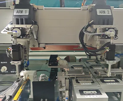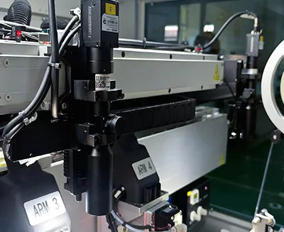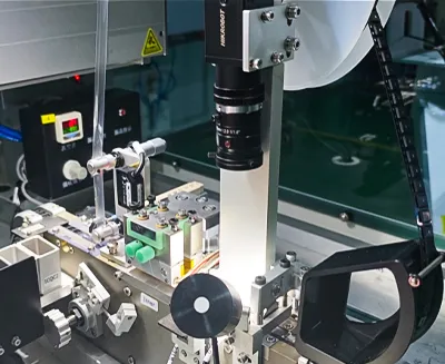
The SCM2000W supports WLCSP chips, enabling eSIM production and laying the foundation for GSMA SAS-UP certification.

Equipped with 2 sets of feeders, supporting inputting by 8mm&12mm wide carrier tapes;
Reject materials are automatically cut for easy recycling.

Four sets of mechanical arm, each with four-axis X/Y/Z/R motion capabilities, equipped with pressure controlling and vision positioning to achieve zero chip damage;
During handling process, the direction of chip pin conversion is adjusted simultaneously;
Compatible with different chip specifications by changing the suction nozzle, supporting a minimum chip size of 1×1mm.

32 encoding stations + 8 verification stations, supporting multi-protocol data writing and electrical performance testing
Dual-switch clamping mechanism for synchronous transmission, improving overall efficiency;
The data system supports online card replacement, ensuring production continuity and data integrity.

20W fiber laser marking machine, providing clear and durable markings;
Sealed dust-free structure, eliminating dust pollution,ensuring long-term equipment stability.

Equipped with 7 vision cameras in total, enabling functions such as chip positioning, OCR inspection, and chip appearance defect detection;
Ensures each chip is traceable and verifiable.

Supports 8mm and 12mm tape widths and 7" or 13" material tray diameters.
Equipped with an initial inspection station that allows operators to conveniently perform offline inspection of finished materials, ensuring consistent output quality.
| Maximum Throughput | WLCSP11-2.5×2.7 2500 UPH QFN8-5×6 2500 UPH |
| Dimension | 2200×1300×1700mm |
| Weight | 1700kg |
| Power Supply | 220V(-5%~+10%), 50Hz, 3.5KW |
| Noise | ≤65dB |
| Operating Temperature | 23℃±3℃ |
| Working Humidity | 50±10%rh |
| Air Supply | Pressure: 0.5 MPa Flow Rate: 500 L/min |
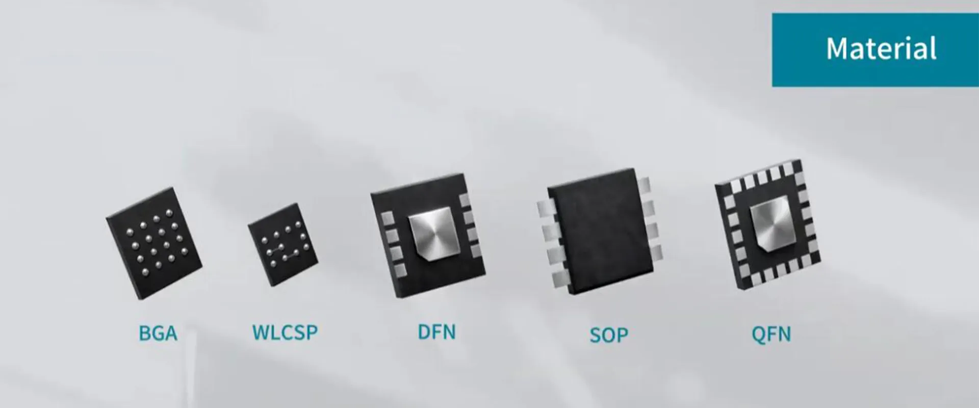
| Applicable Package Types | WLCSP11-2.5 × 2.7; QFN8-5 × 6; Expandable to support DFN, QFN, and WLCSP chip packages with sizes ranging from (2 × 2) mm to (5 × 6) mm, with corresponding KIT components required for additional configurations. |


_00.webp)
The minimum support 2mmX 2mm (LxW) chip high-speed personalized production;
The ultra-small WLCSP chip is the main personalized production object, and can be compatible with chips of various packaging forms such as QFN and DFN.


_00.webp)
For 2mm x 2mm WLCSP chips, the maximum production capacity of the device can reach 2,500UPH.
The IC encoding mechanism is configured with 32 encoding stations and readers and the personalization time is less than 46 seconds, the device capacity can always be maintained at 2,500UPH.


_00.webp)
The pressure detection function designed for "thin, brittle and small" WLCSP chip can effectively prevent the chip from being damaged by excessive pressure during transferring.


_00.webp)
High order exchange efficiency: chip order switching of different package specifications can be completed within 1 hour;
The KIT replacement process is convenient and fast: the position of the mechanism is automatically calibrated through the visual system, and the physical position of the mechanism is not manually adjusted after the replacement of the KIT.


_00.webp)
The new generation PT300 series reader based on FPGA architecture is equipped with stronger performance and more stable work, supporting multi-protocol serial encoding, and can be extended to support the test of various contact electrical performance indicators such as open short circuit and leakage current.


_00.webp)
During the chip transfer process, the vision system collects the precise position of the chip and the target point in real time, and ensures the high accuracy and operation stability of the chip transfer through high-speed real-time displacement calculation.

.webp)
_00.webp)
The chips are all placed inside the equipment, which is not easy to touch at will, and the production process fully meets the requirements of various safety qualifications.
Multiple sets of vision systems are configured to monitor the entire process of chip transportation and the accuracy of data throughout. Moreover, the sequence of chips is detected by the visual system before and after taping to ensure data security during the production process.


_副本.webp)
The chip is laser etched in a closed area to effectively absorb laser dust.


Contact Piotec for Smart Card Solution


